If you’ve followed semiconductor or AI news in the past year, three letters keep popping up: HBM. SK Hynix’s stock doubles. Samsung pours billions into a new fab line. NVIDIA can’t get enough supply. And at the center of every headline sits this mysterious acronym — High Bandwidth Memory.
Yet most people, even seasoned investors, struggle to explain what HBM actually is, how it differs from ordinary DRAM, or why six stacked silicon wafers could be worth more per gram than gold.
This guide will change that. By the end of this article, you’ll understand exactly what HBM means, how each generation — from HBM1 to the cutting-edge HBM4 — compares in specs and performance, why it’s the single most critical component in the AI semiconductor supercycle, and where SK Hynix, Samsung Electronics, and NVIDIA stand in the global battle for supply.
What Does HBM Mean? A Plain-English Definition
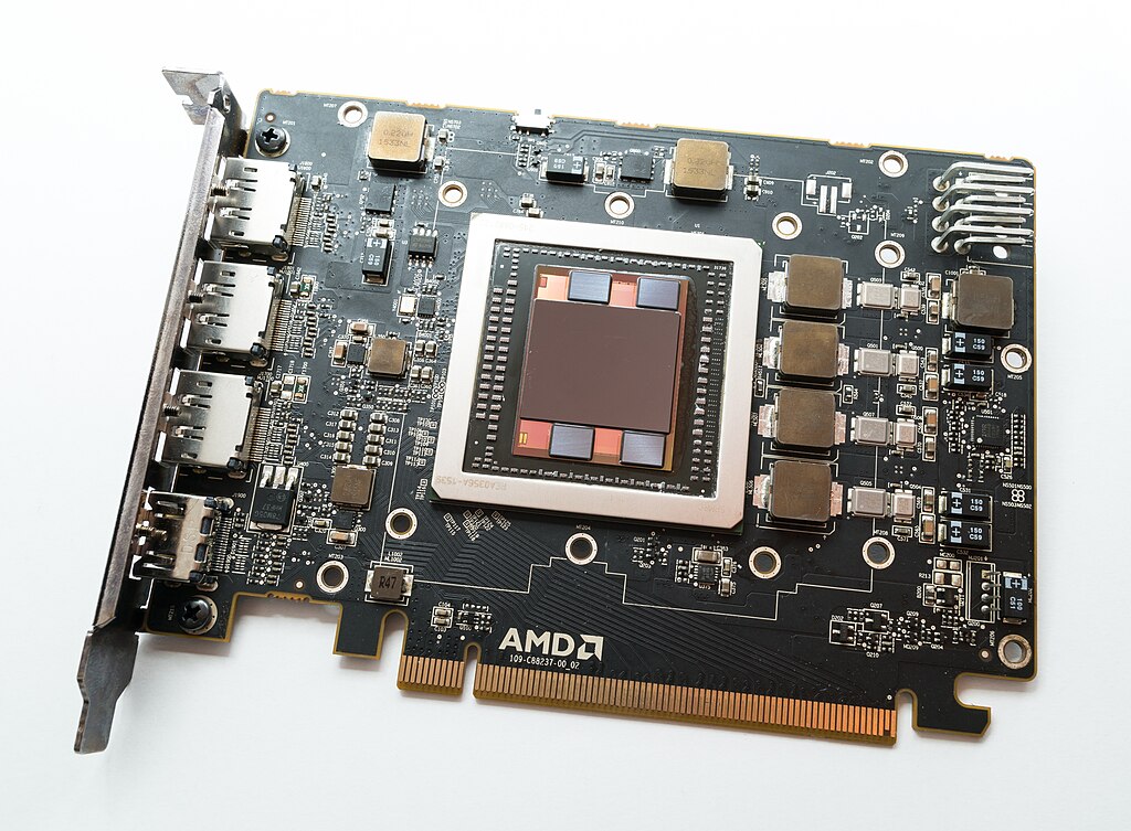
HBM stands for High Bandwidth Memory. It is a type of 3D-stacked synchronous DRAM (SDRAM) designed to deliver dramatically more data per second to processors — GPUs, AI accelerators, and high-performance CPUs — than conventional memory (Source: JEDEC JESD235 Standard).
Think of it this way:
- Regular DRAM (like DDR5 in your laptop) is a single-lane country road. Data moves in one direction at a moderate speed.
- HBM is a multi-story expressway stacked vertically — imagine 8 to 16 floors of highway lanes, all operating simultaneously, connected by thousands of tiny “elevators” (called Through-Silicon Vias, or TSVs).
The result? Bandwidth jumps from roughly 50 GB/s (DDR5 single channel) to over 1 TB/s (HBM3E) — a 20× increase — while consuming significantly less power per bit transferred.
Key Takeaways
- HBM = High Bandwidth Memory, the fastest DRAM standard available
- Uses 3D die-stacking and TSV technology instead of spreading chips across a flat PCB
- Developed initially by AMD and SK Hynix starting in 2008, standardized by JEDEC in 2013
- Current top manufacturers: SK Hynix, Samsung Electronics, Micron Technology
How HBM Works: The TSV Packaging Technology Behind It
Understanding HBM’s secret sauce requires understanding one key technology: TSV (Through-Silicon Via).
What Is TSV?
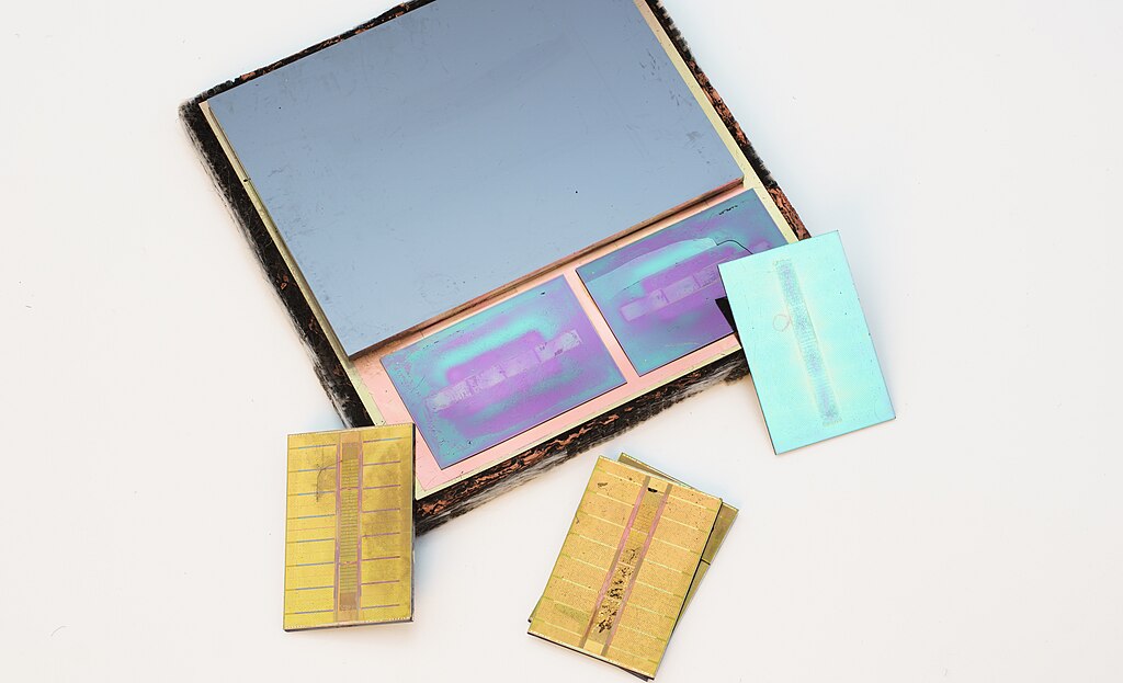
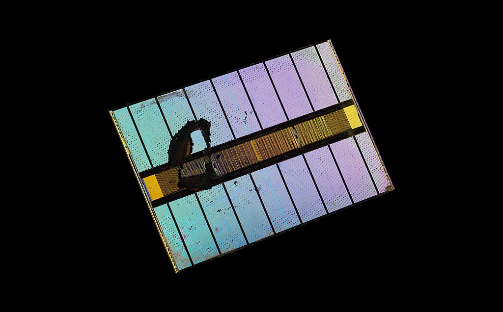
A Through-Silicon Via is a tiny vertical electrical connection — essentially a microscopic copper pillar — that passes directly through a silicon die. Instead of routing signals around the edges (as traditional memory does), TSVs create thousands of direct pathways between stacked DRAM layers.
How the Stack Comes Together
- Individual DRAM dies are manufactured — each one thinned down to about 30 micrometers (thinner than a human hair)
- TSV holes are drilled through each die and filled with copper
- Dies are stacked vertically — 4, 8, 12, or even 16 layers high
- Microbumps bond each die to the next, aligning the TSVs across every layer
- The completed stack sits on a silicon interposer — a bridge chip that connects HBM to the processor (GPU/CPU)
This architecture provides a 1024-bit-wide data bus (2048-bit in HBM4) — vastly wider than DDR5’s typical 64-bit channel. More lanes = more data = more bandwidth.
Why does this matter economically? Manufacturing TSVs and ultra-thin die stacks requires cutting-edge equipment from companies like ASML and advanced packaging from TSMC. The yield rates are notoriously difficult to master — which is exactly why only three companies in the world can mass-produce HBM at scale.
(Source: SK Hynix — HBM3 Announcement, October 2021; IEEE ISSCC 2014 — HBM Technical Paper)
HBM Generations: From HBM1 to HBM4 — A Complete Comparison
HBM has evolved rapidly since its first JEDEC standardization in October 2013. Each new generation delivers more bandwidth, higher capacity, and greater energy efficiency. Here is the complete evolution:
HBM Specification Comparison Table
| Generation | JEDEC Standard | Max Data Rate/Pin | Bus Width/Stack | Max Capacity/Stack | Max Bandwidth/Stack |
|---|---|---|---|---|---|
| HBM1 | Oct 2013 | 1.0 Gb/s | 1024-bit | 4 GB | 128 GB/s |
| HBM2 | Jan 2016 | 2.4 Gb/s | 1024-bit | 8 GB | 307 GB/s |
| HBM2E | Aug 2019 | 3.6 Gb/s | 1024-bit | 24 GB | 461 GB/s |
| HBM3 | Jan 2022 | 6.4 Gb/s | 1024-bit | 24 GB | 819 GB/s |
| HBM3E | May 2023 | 9.8 Gb/s | 1024-bit | 48 GB | 1,229 GB/s |
| HBM4 | Apr 2025 | 8 Gb/s | 2048-bit | 64 GB | 2,048 GB/s |
Let’s walk through each generation:
HBM1 (2013–2015): The Pioneer
The original HBM standard delivered 128 GB/s per stack at 1.0 Gb/s per pin — revolutionary for its time. Development was led by AMD and SK Hynix, with AMD’s Radeon R9 Fury X (June 2015) becoming the first GPU to use HBM commercially.
Key stats:
- 4-die stack (4-Hi), up to 4 GB per stack
- 1024-bit bus width
- First JEDEC standard: JESD235, October 2013
HBM1 proved the concept worked. But its limited capacity (4 GB max per stack) kept it niche.
(Source: AnandTech — AMD Radeon R9 Fury X Review, July 2015)
HBM2 (2016–2018): Entering the Data Center
HBM2 doubled the pin transfer rate to 2.4 Gb/s and capacity to 8 GB per stack. Samsung began mass production in January 2016, and NVIDIA’s Tesla P100 became the first data-center GPU to use HBM2 — signaling the technology’s move beyond gaming into AI and HPC.
Key stats:
- Up to 8-die stacks, 8 GB per stack
- 307 GB/s maximum bandwidth
- First product: NVIDIA Tesla P100 (April 2016)
(Sources: Samsung — HBM2 Mass Production Announcement, January 2016; JEDEC — JESD235a Standard, January 2016)
HBM2E (2019–2021): The Speed Upgrade
HBM2E pushed pin speeds to 3.6 Gb/s (SK Hynix) and introduced 12-die stacks with up to 24 GB capacity. This was the generation that enabled large-scale AI training on GPUs like AMD’s Instinct MI250.
Key stats:
- SK Hynix: 3.6 Gb/s, 460 GB/s per stack (mass production July 2020)
- Samsung “Flashbolt”: 3.2 Gb/s, 410 GB/s per stack
- 12-Hi stacks for 24 GB capacity
(Sources: SK Hynix — HBM2E Mass Production, July 2020; Samsung — HBM2E Flashbolt Announcement)
HBM3 (2022–2023): The AI Inflection Point
This is where the story gets explosive. HBM3 doubled the channel count from 8 to 16 independent channels and the data rate to 6.4 Gb/s, delivering 819 GB/s per stack. SK Hynix was the sole supplier for NVIDIA’s H100 GPU — the chip that powered the ChatGPT revolution.
Key stats:
- 16 channels of 64-bit each (1024-bit total)
- Up to 24 GB per stack (12-Hi)
- NVIDIA H100: 5 HBM3 stacks × 16 GB = 80 GB, 3 TB/s total bandwidth
Why this generation mattered for the market:
When OpenAI launched ChatGPT in November 2022, demand for NVIDIA’s H100 GPUs exploded overnight. Each H100 required five HBM3 stacks — and SK Hynix was the only company qualified to supply them. This single-source dynamic turned HBM into one of the most supply-constrained components in the global semiconductor supply chain.
(Sources: SK Hynix — First HBM3 Supply to NVIDIA, June 2022; JEDEC — HBM3 Standard, January 2022; ServeTheHome — NVIDIA H100 Architecture at Hot Chips 34, August 2022)
HBM3E (2024–Present): The Current King
HBM3E is the current production standard. It pushes the data rate per pin to 8–9.8 Gb/s, cracking the symbolic 1 TB/s barrier per stack. This is the generation powering NVIDIA’s Blackwell B200 and GB200 GPUs.
Key stats:
- SK Hynix: 8 Gb/s, 1 TB/s per stack — mass production March 2024
- Micron: 9.6 Gb/s, 1.2 TB/s per stack — mass production February 2024
- Samsung “Shinebolt”: 9.8 Gb/s — mass production 2024
- 12-Hi and 16-Hi configurations available (36–48 GB per stack)
Competitive landscape:
- SK Hynix maintains a dominant market share in HBM3E, estimated at over 50% of global supply, with all HBM3E orders for NVIDIA’s Blackwell GPUs reportedly fulfilled first
- Micron re-entered the race aggressively, claiming industry-best power efficiency
- Samsung faced quality validation delays with NVIDIA but has been ramping volumes through 2025
SK Hynix’s 12-layer HBM3E entered mass production in September 2024, and 16-layer samples were sent to NVIDIA by early 2025.
(Sources: SK Hynix — HBM3E Volume Production, March 2024; Micron — HBM3E Volume Production, February 2024; Tom’s Hardware — NVIDIA Blackwell B200 Announcement, March 2024; SK Hynix — 12-Layer HBM3E, September 2024)
HBM4 (2025–2026): The Next Frontier
HBM4 represents a fundamental architectural shift. The bus width doubles from 1024-bit to 2048-bit, and DRAM die densities jump to 24Gb or 32Gb — enabling up to 64 GB per stack and a stunning 2 TB/s bandwidth.
Key stats:
- JEDEC JESD270-4 standard finalized: April 2025
- Max bandwidth: 2,048 GB/s (2 TB/s)
- 2048-bit interface (32 channels × 64-bit)
- Up to 16-Hi stacks with 64 GB capacity
- Backward compatible with HBM3 controllers
- Samsung, SK Hynix, and Micron all contributed to the standard
Notably, HBM4’s per-pin data rate is 8 Gb/s — actually lower than HBM3E’s peak (9.8 Gb/s). The innovation isn’t speed per pin; it’s the doubled bus width that delivers the massive overall bandwidth increase. This represents a design philosophy shift: wider, not faster.
TSMC’s growing role: TSMC is set to become a critical player in HBM4 by producing the base die (the logic die at the bottom of each stack). This marks a significant change — previously, memory companies handled all layers in-house. HBM4 is blurring the line between memory manufacturing and logic foundry.
AMD’s MI430X is expected to be the first product utilizing HBM4 memory.
(Sources: JEDEC — HBM4 Standard JESD270-4; Tom’s Hardware — JEDEC HBM4 Standard Finalized, April 2025; JEDEC — HBM4 Preliminary Announcement, July 2024)
Why AI Needs HBM: The Memory Wall Problem
To understand why HBM has become the AI industry’s most critical bottleneck, you need to understand the memory wall — one of the most fundamental limitations in modern computing.
The Memory Wall, Explained
AI models like GPT-4, Gemini, and Llama process trillions of parameters. These parameters must be stored in memory and accessed by GPUs at incredible speed. The GPU’s compute power has been growing exponentially (roughly doubling every 18 months), but memory bandwidth has not kept pace.
This gap is the memory wall. The GPU sits idle, waiting for data — like a Formula 1 car stuck in a traffic jam.
HBM smashes through this wall. By providing 1+ TB/s bandwidth directly adjacent to the GPU (connected via a silicon interposer, not a distant PCB trace), HBM keeps the GPU fed with data fast enough to actually use its compute capability.
Real-World Numbers
Consider NVIDIA’s AI GPU lineup and their HBM requirements:
| GPU | Generation | HBM Type | Total HBM | Total Bandwidth |
|---|---|---|---|---|
| A100 | Ampere (2020) | HBM2E | 80 GB | 2 TB/s |
| H100 | Hopper (2022) | HBM3 | 80 GB | 3.35 TB/s |
| B200 | Blackwell (2024) | HBM3E | 192 GB | 8 TB/s |
| B300 | Blackwell Ultra (2025) | HBM3E 12-Hi | 288 GB | 12 TB/s |
Each generation demands more HBM stacks and faster HBM generations. A single NVIDIA B200 GPU uses eight HBM3E stacks. A DGX B200 server with eight GPUs contains 64 HBM stacks. A hyperscaler building a 100,000-GPU cluster needs 6.4 million HBM stacks.
This is why HBM is the money chip. The demand curve is near-vertical, and supply expansion takes 18–24 months of capital expenditure and yield optimization.
The Economics: Why HBM Is the Semiconductor Supercycle’s Biggest Winner
HBM Revenue Is Exploding
The HBM market has experienced what analysts call an unprecedented demand curve. According to Sourceability, DRAM prices (including HBM) have seen compounded increases exceeding 200% since early 2025, driven overwhelmingly by AI demand (Source: Sourceability — Memory Price Tracking, 2026).
A critical dynamic: HBM crowds out commodity DRAM. Micron has noted a 3-to-1 conversion ratio — every wafer allocated to HBM production removes three wafers’ worth of standard DDR5 capacity. This means HBM demand doesn’t just raise HBM prices; it tightens the entire memory market.
Who Dominates? The Big Three
The HBM market is an oligopoly controlled by three companies:
- SK Hynix — The unquestioned leader. First to mass-produce HBM3 and HBM3E. NVIDIA’s primary HBM supplier. SK Hynix’s HBM revenue has been the single biggest driver of its record profits.
- Samsung Electronics — The world’s largest memory chip maker by total capacity. Samsung initially trailed in HBM3E qualification with NVIDIA but has been aggressively ramping production. Samsung’s strategic priority is closing the HBM technology gap with SK Hynix.
- Micron Technology — The American challenger. Micron surprised the market by achieving HBM3E mass production even before SK Hynix in February 2024, claiming the best power efficiency in the industry.
Why Korean Companies Lead
South Korea’s dominance in HBM isn’t accidental. Both SK Hynix and Samsung have:
- Decades of DRAM manufacturing expertise — HBM is still fundamentally DRAM
- Massive capital expenditure budgets — Samsung alone invested over $50 billion in semiconductor capex recently
- Proximity to the TSV and packaging supply chain — Advanced packaging fabs are concentrated in South Korea and Taiwan
- Deep co-development relationships with NVIDIA — SK Hynix and NVIDIA have been collaborating on HBM since the H100 era
This is why South Korea’s monthly export data — particularly semiconductor exports — has become a bellwether indicator for the global AI trade cycle.
HBM Investment Outlook: What Investors Should Watch
For investors eyeing HBM-related stocks, here are the key factors to monitor:
1. NVIDIA’s GPU Roadmap Dictates HBM Demand
Every new NVIDIA GPU generation requires more HBM per chip. Watch NVIDIA’s product launches and datacenter revenue — they’re the clearest demand signal.
2. HBM Qualification Cycles
Not every company can supply HBM to NVIDIA or AMD. The qualification process takes 6–12 months. Samsung’s delays in HBM3E qualification with NVIDIA directly impacted its competitiveness. Monitor supplier qualification announcements closely.
3. Capacity Expansion Timelines
Building new HBM packaging lines takes 12–24 months. When SK Hynix or Samsung announce new fab investments, the market impact won’t materialize until years later. The gap between demand and supply is the profit driver.
4. The DRAM Price Cycle
Because HBM cannibalizes standard DRAM capacity (the 3:1 ratio), HBM demand lifts prices across the entire memory market. Track trade balance data and memory spot prices on platforms like DRAMeXchange (TrendForce).
5. Geopolitical Risks
US-China semiconductor export controls, potential tariffs, and supply chain diversification efforts all affect HBM supply chains. The concentration of advanced packaging in Taiwan (TSMC) and South Korea (SK Hynix, Samsung) makes this a geopolitically sensitive industry.
Key HBM-Related Stocks to Watch
| Company | Ticker | Role in HBM |
|---|---|---|
| SK Hynix | 000660.KS | #1 HBM producer, NVIDIA’s primary supplier |
| Samsung Electronics | 005930.KS | #2 HBM producer, aggressive ramp-up |
| Micron Technology | MU | #3 HBM producer, power efficiency leader |
| NVIDIA | NVDA | Largest HBM consumer (GPU buyer) |
| TSMC | TSM | HBM4 base die manufacturer |
| AMD | AMD | HBM co-inventor, GPU customer |
| ASML | ASML | EUV lithography equipment supplier |
Conclusion: HBM Is the Backbone of the AI Economy
HBM is not just another memory chip — it is the physical bottleneck that determines how fast AI can scale.
Here’s what to remember:
- HBM (High Bandwidth Memory) solves the memory wall problem by stacking DRAM dies vertically using TSV technology, delivering bandwidth orders of magnitude above standard DRAM
- Each generation — from HBM1’s 128 GB/s to HBM4’s 2 TB/s — has been an exponential leap in both capability and economic value
- The AI semiconductor supercycle is fundamentally an HBM supercycle: every AI GPU requires more HBM, and supply cannot keep up with demand
- SK Hynix leads, Samsung is catching up, and Micron is the underdog contender — together, they form one of the tightest oligopolies in tech
- South Korea sits at the epicenter of this megatrend, making Korean semiconductor exports one of the most important macro indicators in the world
The companies that can stack silicon higher, bond it tighter, and ship it faster will define the next decade of AI. HBM is where the silicon meets the money.
Start Tracking the AI Semiconductor Supercycle
Want to stay ahead of the HBM and AI chip market? ECONPLEX provides real-time tracking of the key indicators and stocks that drive this sector:
- 📊 Track South Korea’s semiconductor export data → — the #1 bellwether for global AI chip demand
- 📈 Follow SK Hynix → | Samsung → | NVIDIA → — Real-time stock data and analysis
- 📖 Explore our Economic Glossary → — Learn every financial term you need to navigate markets
Bookmark ECONPLEX and never miss a beat in the AI investment revolution.
Sources & References
- JEDEC — JESD235 High Bandwidth Memory Standard (October 2013): jedec.org
- JEDEC — HBM3 Standard JESD235C (January 2022): jedec.org
- JEDEC — HBM4 Standard JESD270-4 (April 2025): jedec.org
- Tom’s Hardware — “JEDEC finalizes HBM4 memory standard” (April 2025): tomshardware.com
- SK Hynix — HBM3 Supply to NVIDIA (June 2022): skhynix.com
- SK Hynix — HBM3E Mass Production (March 2024): skhynix.com
- SK Hynix — 12-Layer HBM3E Production (September 2024): skhynix.com
- SK Hynix — HBM2E Mass Production (July 2020): skhynix.com
- Samsung — HBM2 Mass Production (January 2016): samsung.com
- Samsung — HBM2E Flashbolt: samsung.com
- Samsung — HBM3E Shinebolt (October 2023): samsung.com
- Micron — HBM3E Mass Production (February 2024): micron.com
- Sourceability — Memory Price Tracking (2026): sourceability.com
- ServeTheHome — NVIDIA H100 at Hot Chips 34 (August 2022): servethehome.com
- Tom’s Hardware — NVIDIA Blackwell B200 (March 2024): tomshardware.com
- AnandTech — AMD Radeon R9 Fury X Review (July 2015): anandtech.com (archive)
- IEEE ISSCC 2014 — HBM Technical Paper: doi.org
- Wikipedia — High Bandwidth Memory: wikipedia.org
- JEDEC — HBM4 Preliminary Specification (July 2024): jedec.org
Image credits: All photographs by Fritzchens Fritz via Wikimedia Commons (CC0 Public Domain).